Connect with us

Tech

Samsung Vs TSMC: Race For 3nm Chip Development

Published

on


Recently TSMC has announced that it will go ahead and work on producing a 2nm memory chip by 2025 to be the forerunner in the foundry and memory chip business. This move is to rival Samsung, which also announced in April this year that it will work on 2 nm by 2025.

Before this, Samsung also informed in April that it would start to work on the 3nm chips 3GAE (3 nm-class gate-all-around early) fabrication process, starting in mid-2022.

TSMC is expected to mass-produce the first-gen 3nm chips (N3) for its customers in early 2023 & 2nm by 2025. TSMC informed at TSMC Technology Symposium 2022 this Thursday.

However, before developing the 2nm technology, the TSMC will use advanced 3nm fabrication processes N3P, N3S, and N3X to produce a 3nm chip between 2023 and 2025. 18 This will result in an 18% percent performance increase at the same power while reducing power consumption to 34% if computing is kept consistent.

Intel also announced to reenter manufacturing business with a whopping 80B dollar investment in Arizona and Ohio last year and plans to work on the 1.8nm process starting 2025. 

Intel, Samsung, and TSMC are the only competent players in this business for mass production.

Although Samsung and intel are longtime rivals and friends at certain times, Intel has collaborated with TSMC but doesn’t want to share all its prowess in the foundry business with it, while Samsung is trying to outdo TSMC and Intel trying to enter the manufacturing business it seems a likely alliance could form as both can benefit from each other.

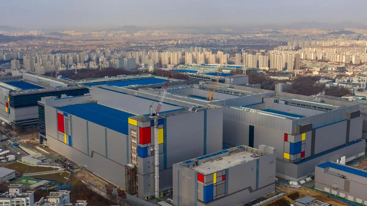
Samsung has likely got an advantage this time due to using a more advanced GAAFET (gate-all-around field-effect transistor) architecture compared to TSMC’s FinFET (fin field-effect transistor). Samsung will become the first manufacturer of semiconductors to start using gate-all-around field-effect transistor (GAAFET) architecture with its upcoming 3 nm fabrication process. 

Samsung claims the process would enable a 30% performance increase, a 50% power consumption reduction, and up to 80% higher transistor density.

Another development favoring Samsung could be the meeting between Samsung & Intel’s President & CEO.respectively.

After visiting the DAVOS forum in Switzerland, Intel CEO Pat Gelsinger met with Samsung vice-chairman Lee Jae Yong in the Samsung Seocho building in Seoul. Pat also visited several officials of Samsung, including the Co-Ceo and head of Samsung mobile. This meeting took place 10 days after the US president’s visit to S.Korea to Samsung’s electronic plant on May 20.

Targeting to produce at a mass level with wide reach, Samsung has both capability and will to make a market out of this, as we have seen before in many criteria. Also, not forget the recent CXL-based memory development by Samsung and collaborations with IBM, Intel, Montage Technology, AMD & others.

While this business is completely dominated by these three, the Chinese Semiconductor manufacturing Int, Co. also wants to compete. Japanese are working with the US on 2nm to complete by 2025.

The chipmaking tech is extremely difficult to put a complex process requiring precision, clean environments, expensive factory equipment, and time. It takes GlobalFoundries three months on average to engrave and transform mirror-smooth silicon wafers into layered semiconductors, not to mention the lower the nm(nanometer) more difficult it becomes to fit the no. of transistors in a wafer-thin silicon layer.

So, a lower nm transistor means less power is required for it to work. Lower power consumption makes a huge difference overall when you look at all the transistors in a CPU. It makes your processor more power-efficient than a higher nm processor with larger transistors.

Although TSMC has had superiority over Samsung, this time, Samsungs seems to show a promising future.

To learn more about this news, previous developments, and the mentioned technology, refer to the links below.

Sources & References:


Harsh is a seasoned technology enthusiast with a deep passion for Android. Since its announcement in 2007, he has closely followed the evolution of this operating system, gaining a comprehensive understanding of its features and capabilities. His background in Android, IT, and Journalism has equipped him with the skills to analyze and present complex technological concepts in a clear and engaging manner. As the Editor-in-Chief at Samlover.com, Harsh is dedicated to sharing his knowledge and experiences about Android, services, and applications with the world.

Tech

Google And Samsung Partnering Together On AI For Android & Galaxy Phones

Published

on


Google and Samsung are coming together as their partnership goes beyond Android. On one side, Pixel smartphone devices use Samsung-manufactured Tensor chips; on the other hand, Smsung’s flagship Galaxy smartphones have AI features, like Circle to Search, noticeably before even the Pixel 8 series got this novelty. 

In the report it is being unveiled, Rick Osteroh,  SVP of platforms and devices at Google, stated that the brand’s “partnership has never been stronger.” A post on X shared by @rosterloh pointed to a positive meeting between TM Roh and @SamsungMobile leadership. It highlights a strong partnership between both and excitement about future collaborations, particularly in the area of AI.

Following the statement, he also attached a selfie with TM Roh, president and head of MX Business at Samsung Electronics. 

Then, @SamsungMobile reposted Osterloh’s post and teased that both brands are actively working on expanding the functionalities of AI features for Android and Galaxy devices to enhance Galaxy experiences. 

Google has already announced at the last Galaxy Unpacked event, back in January in San Jose, that the Samsung Galaxy S24 series will use Gemini AI models to power the forthcoming AI capabilities in the applications and services built by the Korean giant. The brand also brought new functionalities for Google Messages and Android Auto, powered by Gemini Nano

For enhancing the summarizing facility, Samsung’s Smarter Notes, Voice Recorder, and Keyboard applications use the AI model Gemini Pro, whereas the Galaxy S24 series smartphones use Imagen 2 text-to-image technology to offer “Generative Edit” features in the Gallery application for upgrading photo editing. 


Continue Reading

Tech

Samsung Laptops Might Embrace Qualcomm’s New Snapdragon X Chip

Published

on


Finally, Qualcomm has debuted its new ARM-based processor, the Snapdragon X Plus, designed for laptops. We anticipate Samsung to incorporate this chipset into its upcoming laptops.

However, this new chipset appears a bit below the company’s high-end laptop chipset, the Snapdragon X Elite, which was unveiled a few months ago and is expected to be used in Samsung’s forthcoming Galaxy Book 4 Edge. 

The Snapdragon X Plus is a 4nm chip with a 10-core CPU. The Snapdragon X Elite and this newly launched chipset use the same Oryon CPU cores. This chipset is expected to be used in more affordable laptops running on the Windows OS. The CPU of this chipset operates at 3.4GHz, while the Snapdragon X Elite clocks at 3.8GHz.

Snapdragon X Plus’ integrated Adreno GPU has 3.8 TFLOPS of power, which could be equivalent to the Intel Core Ultra 7 series. The noticeable thing that remained constant in this new chipset is its NPU, which still offers 45 TOPS performance for on-device AI inference, similar to the Snapdragon X Elite. 

This qualifies the chip as an AI chip, according to Microsoft Copilot’s minimum requirement of 40 TOPS. The brand has assured that the Snapdragon X Plus delivers 10% faster CPU performance than Apple’s M3 chipset while running at the same power. On the other hand, the Snapdragon chip claims to be 37% faster at the same wattage as the Intel Core Ultra 7 155H. This chip is expected to appear in laptops and will debut in the second half of this year. 

Previously, Samsung has used Qualcomm’s top-of-the-line and mid-range Snapdragon chipset in its ARM laptops, and the giant has already unveiled that the forthcoming Galaxy Book 4 Edge will use the Snapdragon X Elite. Given this fact, it is quite possible that the brand could launch a more affordable Galaxy Book 4 series laptop with the Snapdragon X Plus. 


Continue Reading

Tech

Here’s The Key Fact Why UFS 4.0 Memory Just Got Faster

Published

on


The fact is, other storage facilities can’t replace the device’s local storage; it remains an essential factor yet. 

Despite cloud storage, smartphone storage remains crucial, and UFS 4.0 makes phone storage faster than ever before, but the fact is there is always room for improvement. The latest UFS chipsets run at the same speed as an SSD; however, a brand founded by Toshiba has managed to make the UFS 4.0 standard even more efficient. 

Kioxia is a Japanese multinational computer memory manufacturer that develops, produces, and sells flash memory and SSDs, and now it has recently introduced chips that arrive with storage capacities of 256 GB, 512 GB, and 1 TB. 

Kioxia Revs Up UFS 4.0 Memory Standard

The brand has now revealed the THGJFMT1E45BATV, THGJFMT2E46BATV, and THGJFMT3E86BATZ chips that offer 50% faster random writing in an 18% smaller area. The chips have their particular size based on their storage capacities, which are mentioned below:

  • 256GB and 512GB chips: 9.0 x 13.0. x 0.8mm
  • 1TB chip: 9.0 x 13.0 x 0.9mm 

Kioxia has equipped the new UFS 4.0 chips with BiCS Flash 3D NAND, making them 18% smaller as compared to the previously announced 11 x 13mm chips. The write speed of the new UFS chips has been boosted by 15%, and the random write speed has increased by as much as 50%, with a 30% rise in random read speed as well, although the maximum read limit remains unchanged at 4.640 MB/s. 

It is also announced that the production of the 256GB and 512GB variants of these new UFS chips will begin by the end of this month, whereas the 1TB variant will go into production in June.


Continue Reading