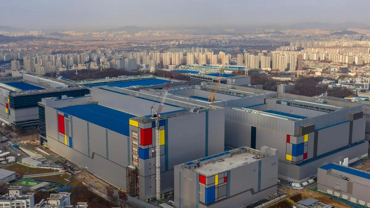
Samsung Foundry has been struggling hard for so long in its HBM business to regain its leading position in the market; however, now it is all set to bounce back with the upcoming HBM4 chipset.
It seems that the struggling days have finally come to an end, as the company’s HBM4 4nm logic dies have reportedly achieved a yield of over 90%, which is truly impressive output. A 90% successful yield rate is quite a promising result for stable mass production, which should attract major clients widely.
The company used its in-house 4nm process for the logic die of HBM4. The logic die is a crucial component that helps to connect the stacked memory to the GPU, placed at the bottom of the HBM, which consists of multiple stacked memory chipsets (DRAMs). It also controls power and data signals.
According to a new report from Chosun, Samsung has now made substantial progress with a yield of over 90%, which suggests the production process has become stable enough for mass production.
A semiconductor industry insider, stated, “Samsung Electronics applied a fine process to the HBM4 logic die ahead of its competitors in order to make up for its slump in the previous generation,” and added, “Although there is still market verification left, it is true that the importance of foundry process technology will be highlighted in the upcoming next-generation HBM market.”
It will be interesting to see what happens next and whether the chipset will be efficient enough for the company to regain its position.