Samsung
Samsung’s Advanced 3D Chip Packaging Paves Way for HBM4 by 2025
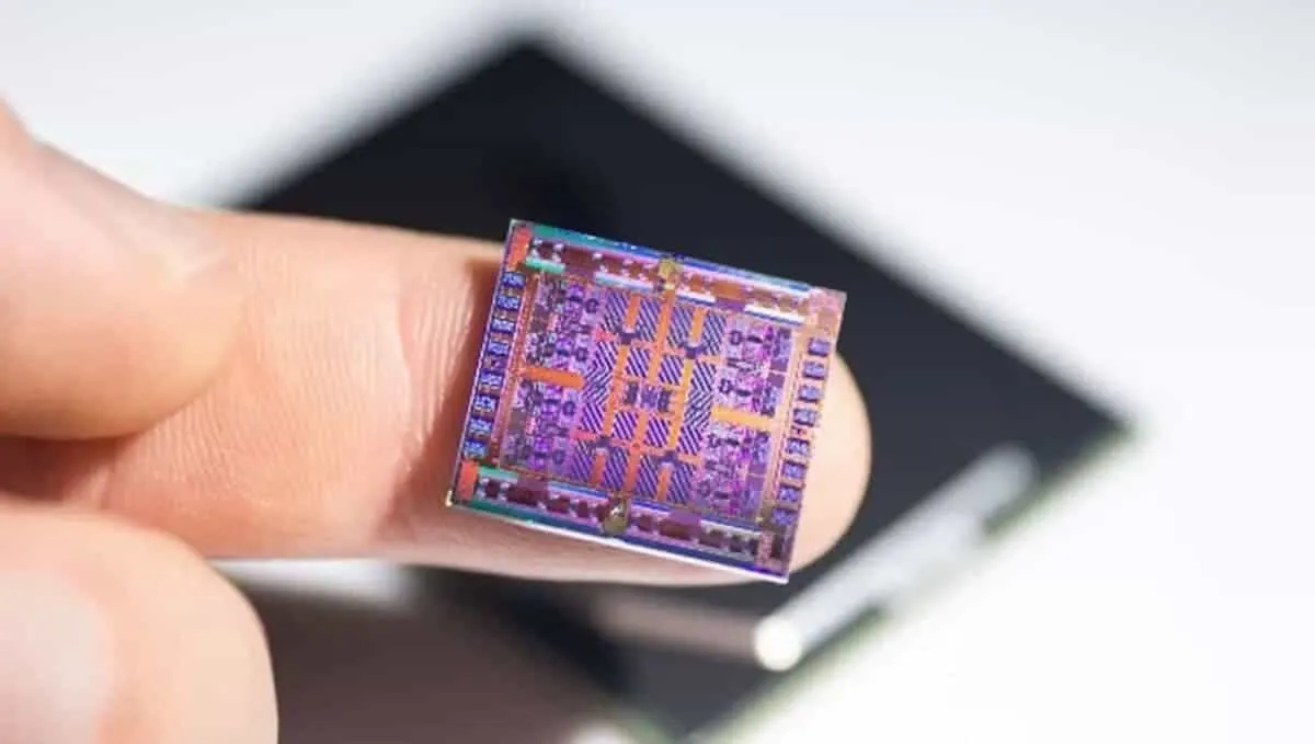
Samsung Electronics is gearing up to launch three-dimensional (3D) packaging services for high-bandwidth memory (HBM) soon.
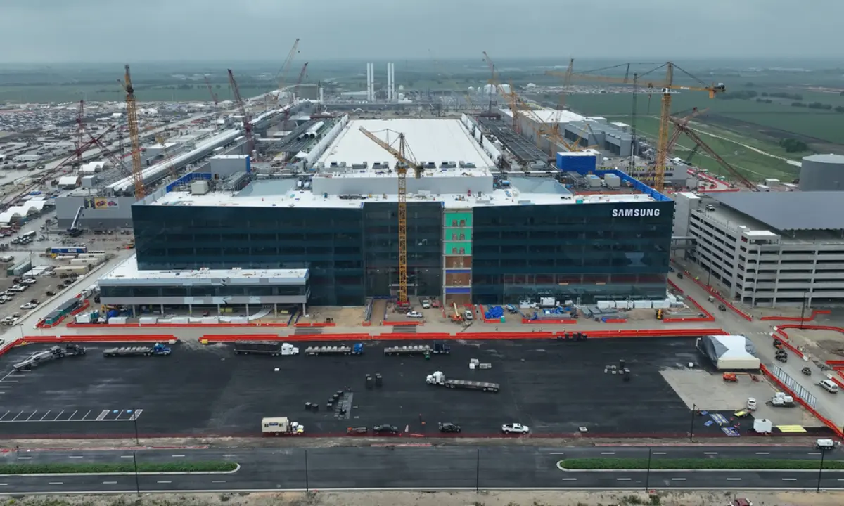
The Korean giant is launching a new 3D packaging technology for high-bandwidth memory (HBM) by the end of this year. This mechanism is expected to be used in the next generation of AI chips (HBM4), which will be released in 2025. At the Samsung Foundry Forum 2024 held in San Jose, California, the world’s largest memory chipmaker unveiled its next-generation chip technology roadmaps.
It’s the initial stage for Samsung to release the 3D packaging technology for HBM chips at a public event. Presently, HBM chips are packaged mainly with 2.5D technology. It arrived nearly two weeks after Nvidia co-founder and Chief Executive Jensen Huang unveiled the new-generation architecture of its AI stage Rubin during a speech in Taiwan. HBM4 will likely be embedded in Nvidia’s new Rubin GPU model, expected to hit the market in 2026.
The Korean giant’s latest packaging technology features HBM chips stacked vertically on top of Samsung Advanced Interconnection Technology-D. The brand is also offering a complete service based on turnkey for the 3D packaging of HBM chips. This involves integrating HBMs from their memory division with GPUs made for other brands by their foundry unit. The 3D packaging offers advantages, such as lower power consumption, faster processing, and improved signal quality.
The Korean giant is also looking forward to debuting a unified package for AI accelerators with all the essential components by 2027. This package will also include optical elements for super-fast data transmission. As per the increasing demand for low-power, high-performance chips, HBM is all set to make up 30% of the DRAM market in 2025, up from 21% this year.