Samsung
Samsung Announces Two-Track Development Plan for HBM Technology
The Korean brand ‘Samsung’ is continuously working on its next HBM iteration and is now looking forward to a two-track approach for its high-bandwidth memory (HBM).
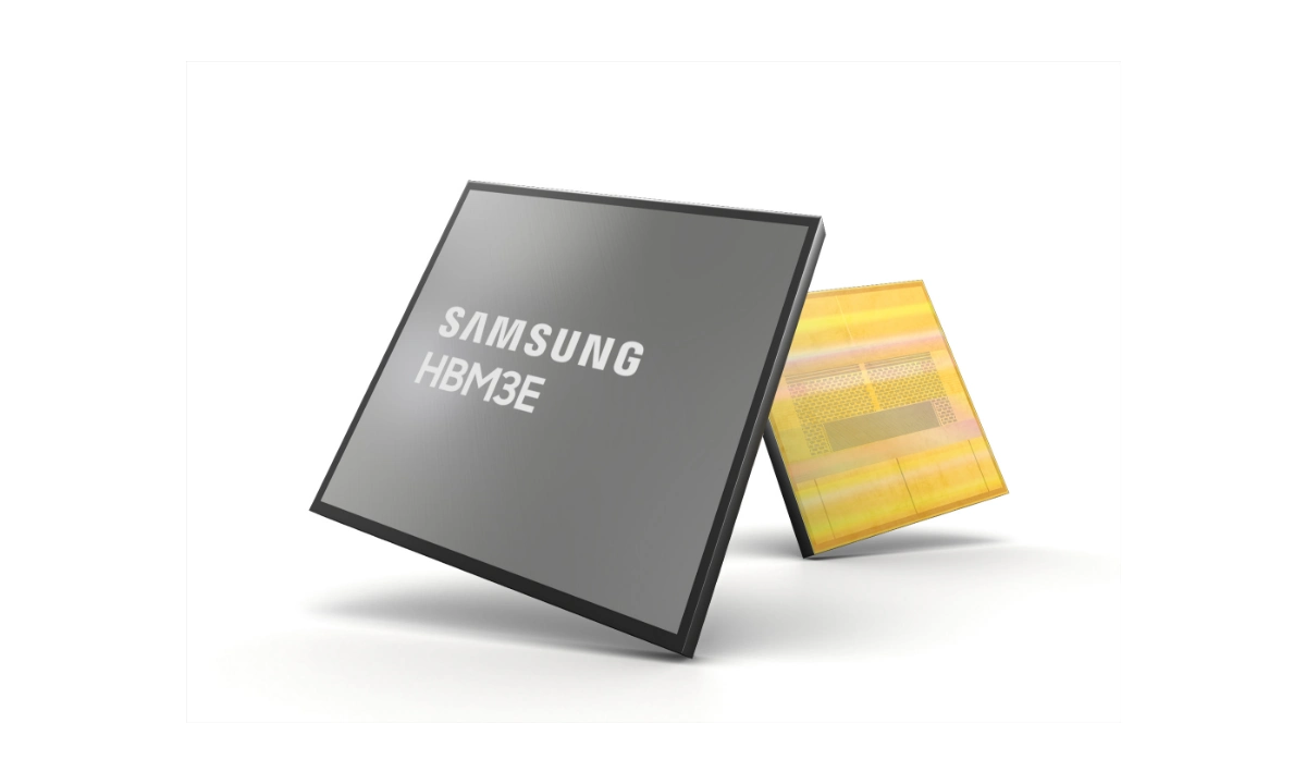
Samsung recently formed the HDM development team, which already moved into a permanent office from a task force in March and is now aiming to develop HBM4. On the other hand, HBM3E is being addressed by Samsung’s existing DRAM design team and is also expected to go into mass production soon.
HBM4 is the sixth-generation iteration of the memory chip, which is in high demand because it is being coupled with AI chips. LeeJung-base, Samsung’s head of its Memory Business, is guiding the HBM development crew. The brand is strengthening the team by reshuffling key staff. For HBM4, Samsung is gearing up to offer samples to customers next year and begin mass production in 2026.
Apart from this, the opponent, SK Hynix, stated that it has also decided to start mass production of an A12-stack HBM4 by the end of 2025. This points out the possibility of Samsung starting its production as soon as possible. The Korean giant disassembled its HBM development team in 2019, which gave SK Hynix an opening to take a huge share of the market through HBM3.
If the reports are to be believed, the brand is convinced it can retake the leadership spot through HBM4 and believes it can make it better than its rival. Plus, the giant thinks it’s a way of making HBM, thermal compression non-conductive film (TC-NCF), from its warpage-resistant qualities, which will permit it to produce HBM with higher stacks as compared to SK Hynix.
Another advanced technology Samsung believes it has is the Samsung Foundry. Starting with HBM4, the logic die on the bottommost layer of the HBM is expected to be made with foundry processes. Rival SK Hynix is planning to partner with TSMC for this.