Connect with us

Samsung

Samsung team explains the ISOCELL HP2 Sensor of Galaxy S23 Ultra’s 200MP camera

Published

on


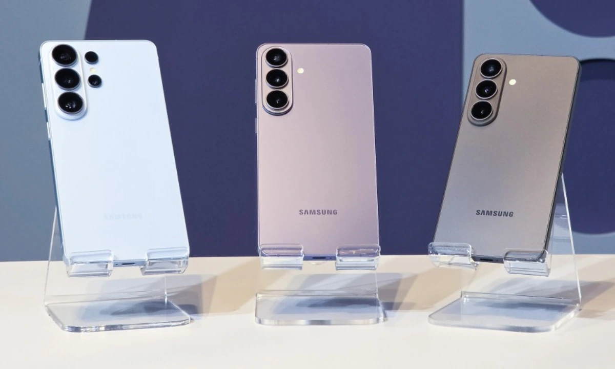
In the latest flagship, the Galaxy S23 series’ top-of-the-line Ultra model (Galaxy S23 Ultra), Samsung features its 200MP image sensor- ISOCELL HP2. It is the first time that Samsung has used this big image sensor in its Galaxy phone. The wonderful thing is this new sensor has been made by Samsung itself, which was a really tough task for the manufacturer. Let’s take a look at the journey of the development of this sensor. 

Informatively, the Galaxy S23 Ultra’s this new advanced camera sensor capable of lending an incredible photography experience. The sensor will open up opportunities for professional and recreational photographers who want to take their photography to the next level. As per Kyungho Lee, the Vice President of the Pixel Development Team, they had dramatically increased the pixel storage capacity of this sensor. 

ISOCELL HP2 200MP Sensor

If you are unaware, the Galaxy S23’s HP2 sensor is capable of capturing pictures in three modes- 12MP, 50MP, and of course, 200MP, depending on their tastes or the lighting conditions. The sensor features Tetra2pixel technology in it that can group 4 or 16 nearby pixels together depending on the lighting condition to produce bright and sharp images even in low-light conditions. 

Let us inform you a new technology named Dual Verticle Transfer Gate has also been developed, which is capable of producing images with no ghosting and a wide dynamic range of brightness. Seungjin Lee from Sensor Design adds he has stated in that manner-

“A significant boost in analog-to-digital conversion (ADC) was crucial. Our developers devised a method to overcome this obstacle and applied it to ISOCELL HP2 for the first time, allowing us to anticipate and correct potential mismatches between ADCs in advance. As a result, we were successful in achieving all of our goals for the image sensor’s performance and reliability.” 

Better results sure require a lot of efforts

However, making such an advanced and complicated product must not be easy, and the company sure faced many problems developing it. At first, Samsung thought that pixel shrinking had reached its limit, but then it continued to advance its ISOCELL technology, believing that there are no limits to creating new and cutting-edge technologies. Kyungho also made a statement in that manner- 

“At Samsung, we devote all these efforts to deliver a camera experience that enables all mobile users to capture their precious moments and priceless events as vividly and clearly as if they were seeing them with their own eyes.” He also said, “As one of the team members who participated in the evaluation process, I would say it is one of the best ultra-high resolution image sensors we have ever released.”

Samsung’s new challenge for PUBG Mobile players: Version 2.5

Informatively, the developer team has achieved ISOCELL’s top-class image quality at the 200MP sensor by dramatically increasing the number of electrons that can be packed into each pixel. This new architecture is capable of reducing noise in both 12MP and 50MP modes and provides outstanding quality in both bright and dark environments. Seungjin has given credit for the sensors’ success to their excellent team and said-

“We were able to meet the deadlines and achieve all the desired performance outcomes by properly allocating focus and resources to high-priority objectives.”

The future will be full of surprises

As such bigger image sensors, specifically sensors with more than 100MP, are currently limited, and we are expanding them to expand with the time being. The South Korean firm is planning to strengthen its market leadership in terms of the ultra-hight resolution image sensor category with the help of its best image sensor lineup, including the 108MP, 200MP, and upcoming ones. Undoubtedly, the future will be full of surprises. 

Nota bene, Kyungho said, “We are aiming for more pixels than the 576 million known to be the maximum effective pixels in the human retina. Soyoon Choi also predicts- 

“If this trend and evolution continue, we’ll see amazing image sensors which perfectly mimic the human eye not only in terms of detail expression but also dynamic range and color reproduction in the near future.”


Harsh is a seasoned technology enthusiast with a deep passion for Android. Since its announcement in 2007, he has closely followed the evolution of this operating system, gaining a comprehensive understanding of its features and capabilities. His background in Android, IT, and Journalism has equipped him with the skills to analyze and present complex technological concepts in a clear and engaging manner. As the Editor-in-Chief at Samlover.com, Harsh is dedicated to sharing his knowledge and experiences about Android, services, and applications with the world.

Samsung

Samsung Receives $6.4 Billion Subsidy From The US Government

Published

on

By


The Korean electronic firm ‘Samsung Electronics’ has just been awarded an efficient grant of up to $6.4 billion by the US government. 

This significant and huge grant aims to help Samsung expand its chip production in Central Texas. The Korean giant has decided to invest approximately $45 billion in constructing and expanding its Texas facilities over the next few years. 

Apart from Samsung, the rest of the tech giants, including TSMCIntel, and Microchip, are receiving incentives from the Department of Commerce. The key reason behind this subsidy is to boost US chip production for critical industries such as defense and autos, as well as avoid dependence on other chipmakers like China and Taiwan. 

The US is planning for its comeback with a bang in chip manufacturing, in which Samsung is playing a key role as the brand is investing a huge amount in US chip production along with the support of the US government. Samsung got this grant under the CHIPS Act. This funding will result in building two new chip factories, a research center, and a packaging facility. 

This collaboration is a good opportunity for both Samsung and the US government to make America a leader again in chip design as well as in advanced manufacturing, research and development, and packaging. The Semiconductor Industry Association (SIA) praises Samsung and the US government’s CHIPS Act incentives. 

Commerce Secretary Gina Raimondo illuminates the importance of this project for raising US technological capabilities and innovation in the semiconductor market.


Continue Reading

Samsung

Samsung Promises Dream Battery For Next-generation Electric Cars

Published

on

By


The Korean electric firm ‘Samsung’ is all set to expand its battery business, as it is promising the dream battery for electric cars. 

The Korean giants are gearing up to add an extra layer to their versatility. Samsung SDI has recently revealed plans to power electric cars with a solid-state battery. Three years from now, in 2027, this battery is to go into lineup production for electric cars, and Samsung speaks of a dream battery. 

Now, the Korean giant is actively working to become the top brand in the global EV battery market. A couple of years ago, back in May 2015, Samsung SDI acquired Magna Steyr Battery Systems gmbH (MSBS), which offered the brand a complete business system for electric vehicle batteries. 

The battery will efficiently lower fire risk as compared to ritual lithium-ion batteries. It packs a punch with an energy density of nearly 450 Wh/kg, potentially leading to longer ranges for electric vehicles. The brand assures that the battery can be charged up to 80% in just nine minutes. 

Lithium-ion batteries from today’s production cars are nearly 200 Wh/kg or lower. Samsung itself, with its recently best battery, is a full 40% down the new solid-state generation. However, there are doubts regarding Samsung’s announcement from experts.


Continue Reading

Samsung

Samsung Boost Exynos GPU & Hiring Developers In The US & India

Published

on

By


Samsung Electronics is concurrently hiring developers in the U.S. and India regions to energize its graphics processing unit (GPU) technology capabilities. 

The Korean Electronics firm stated that it is pursuing talent in several positions, from GPU design to performance advancement, graphics drivers, and application processor (AP) software development, including GPUs. 

The Korean brand is hiring developers at its R&D centers in Austin (SARC) to support its graphics processing unit technology. They are located in Austin, USA, where Samsung Electronics’ R&D center is located (SARC), San Jose (ACL), and Bengaluru, India (SSIR). The aim behind this decision appears to be to upgrade the overall performance of their application processors (AP) by concentrating on the GPU technology within them. 

A semiconductor industry official stated that “the Exynos portfolio of GPUs equipped with GPUs is expanding not only for high-spec but also for mid-to-low-end smartphone APs and automotive APs,” plus “the importance of GPUs for processing high-volume data is gradually expanding.”

Samsung Electronics has not developed its GPUs yet, although its Semiconductor Business Division (DS) GPU development team has partnered with SARC· ACL· It is a part of SSIR and is currently in charge of optimizing GPUs for smartphone APs. GPUs developed in collaboration with AMD are being applied to mobile applications. A few years ago, in 2022, the first AMD GPU named ‘Xclipse’ was installed in the Exynos 2200 chipset. 

Although issues with heat generation as well as performance limitations were boosted along with the Exynos 2200, Samsung has since stepped up its development to regain the reliability and competitiveness of the Exynos. It is expected that the GPU development team at Samsung could work with AMD on next-generation GPU development and performance optimization. 

Via


Continue Reading