Samsung
Samsung Ramps Up 3nm Chip Production to Compete with TSMC
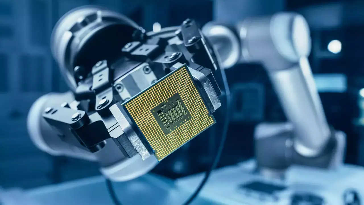
Samsung is eagerly trying to compete with the biggest chip manufacturer, TSMC. To do that, the company has increased the production of the 3nm chip. However, it is still not achieving the same yield rate as TSMC.
According to a tipster, @Teck_Reve, Samsung’s initial yield rate was 10 to 20%, which has now increased by over threefold, but he didn’t mention the exact amount of production increase.
If you don’t know about the yield rate, it is a measure of the usable chips manufactured at a facility. It is calculated as the percentage of the total number of chips produced. If the yield rate is high, the number of defective chips is low. Ultimstrly it mrsdutr the efficiency of the chips production.
The Korean giant has started making 3nm chips in 2022, but it has struggled to achieve the yield rate. It has transitioned from the FinFET transistor architecture to the more advanced GAA architecture, but Samsung hasn’t achieved the desired yield rate while at the same time the TSSMC, with the same 3nm fabrication manufacturing, has achieved the efficiency and has enjoyed the yield.
However, if the report is inaccurate, there are some positive signs that Samsung is trying to fill the gap between the efficiency of manufacturing. As per the tipster, the Korean giant is providing the 4nm chips, which employ the FinFET architecture. The power efficiency and logic area have increased by 20–30%. If this happens, the company will get a major advantage to edge the 3nm semiconductor market.
According to a recent report, Samsung has informed its customers about a rebranding of its 2nd-generation 3nm process. The company will call the 2nm process instead of the 2nd generation 3nm process, technically a 3 nanometer process, but the Korean firm is renaming it to 2nm. It is confusing that the company is taking this step, but the real 2nm chips will be available next year’s second quarter.