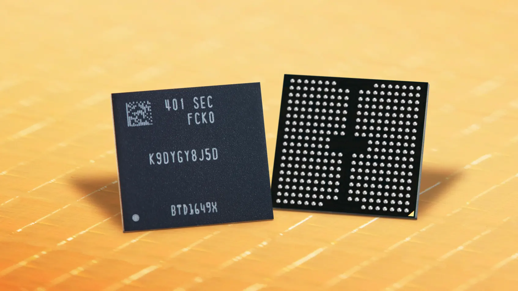
Samsung Electronics Begins Mass Production For 9th-Gen V-NAND

The Korean Electronics firm announced that it has begun mass production for its one-terabit (Tb) tripe-level cell (TLC) 9th-generation vertical NAND (V-NAND).
One of the key reasons for beginning this mass production is just to solidify its leadership in the NAND flash market. This 9th generation V-NAND flash memory has significant improvements. It offers a 50% increase in storage density compared to its predecessor, the 8th-generation V-NAND. This appears due to the tiny cell size and thinner design.
The Korean giant also executed new techniques for upgrading the reliability and lifespan of the memory cells while eliminating dummy channel holes, which significantly reduced the planar area of the memory cells. The Head of Flash Products & Technology of the Memory Business at Samsung Electronics, SungHoi Hur, stated, “Through our latest V-NAND, Samsung will continue to set the trend for the high-performance, high-density solid-state drive (SSD) market that meets the needs of the coming AI generation.”
Samsung‘s advanced ‘channel hole etching’ technology exhibits the brand’s leadership in process capabilities. This technology creates electron pathways by stacking mold layers and increases fabrication productivity as it authorizes simultaneous drilling of the industry’s highest cell layer count in a double-stack structure. As the cell layers increase, the capability to pierce through higher cell numbers becomes crucial, demanding more complicated etching techniques.
The 9th-generation V-NAND is enabled with the next-gen NAND flash interface, Toggle 5.1, which will help to support the increased data input and output speeds by at least 33% to up to 3.2 Gbps. The Korean giant plans to solidify its position within the high-performance SSD market by expanding support for PCIe 5.0.
With the advancement in low-power design, power consumption has also improved by 10%.


